|
|
Post by MadModder on Oct 1, 2006 13:02:13 GMT -5
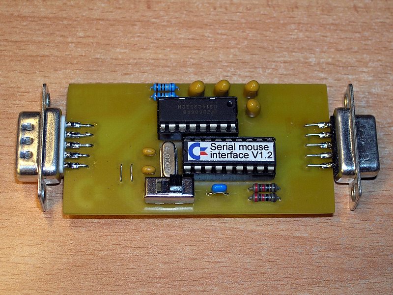
I just finished building the interface. Idea and original design by Levente Hársfalvi. 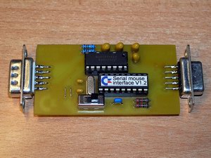 Do you recognise that little switch?  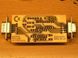  The switch is for selecting 1350/1351 mode (digital/propotional) It works pretty good, but the movement of the sprite pointer is not as smooth as I remember it was with a real C1351. And the way the 1351 protocol works, you get a pointer that jerks around all over the screen if you move the mouse too fast. That happens quite easy with this. Oh well. It's better than nothing. |
|
|
|
Post by gmoon on Oct 1, 2006 14:57:04 GMT -5
Your PCBs are always beautiful--what's your secret?
Do you use presensitized boards?
|
|
|
|
Post by MadModder on Oct 2, 2006 12:19:30 GMT -5
Hmm... presensitized? Sensitive to light... Yes I use boards that have a layer of UV sensitive coating. If that is what you mean. I always manually route the layout. Autorouter really sucks on single sided boards. Then I print the layout on OH film with a laserprinter, and place the film on top of the board, and then glass on top of that. And some weights. Then I expose the whole thing to 300W of UV light in 7 minutes. After that some development in sodium hydroxide, and then etching in sodium.. uhm.. sulphate? Works every time. |
|
|
|
Post by gmoon on Oct 2, 2006 12:34:20 GMT -5
Hmm... presensitized? Sensitive to light... Yes I use boards that have a layer of UV sensitive coating. If that is what you mean. Yep. Looks like a winner. Again, nice job. |
|
|
|
Post by MadModder on Oct 2, 2006 14:16:04 GMT -5
Thanks.
|
|
|
|
Post by gmoon on Oct 3, 2006 7:44:22 GMT -5
I always manually route the layout. Autorouter really sucks on single sided boards. Then I print the layout on OH film with a laserprinter, and place the film on top of the board, and then glass on top of that. And some weights. Then I expose the whole thing to 300W of UV light in 7 minutes. After that some development in sodium hydroxide, and then etching in sodium.. uhm.. sulphate? Works every time. I ordered some pre-coated boards yesterday  . I should be all set for the production process--I've got a full darkroom downstairs (which doesn't get used much now in the digital photography age.) For years I've been working on & off with alternative photographic methods, usually gum dichromate. So making full size contact negatives (or positives) is no problem. I have some large graphic arts film (kodalith) and print frames. Hopefully I won't need any of that stuff but my sunlamps (UV) and the contact printing frames. I understand that an inkjet transparency doesn't have the image density neccesary, and a laserprinter must be used....with luck the litho film won't be needed. |
|
|
|
Post by MadModder on Oct 3, 2006 12:20:12 GMT -5
Previously I used an inkjet printer. I had to print two copies, and tape them ontop of each other to get it black enough to block the light.
I actually even have to do that with my laser printouts...
|
|
|
|
Post by gmoon on Oct 3, 2006 15:19:55 GMT -5
O.K., that's good to know.
I'll make some tests with my UV lamps; their wavelengths could make a difference, just like the opacity of the image. At least one lamp is mercury vapor, and kicks out lots of UV.
|
|
|
|
Post by gmoon on Nov 18, 2006 12:25:01 GMT -5
Picking up a on a project that's been 'hanging' for two months, my first attempt w/positive resist PCBs was a success! (and my wife's at a conference so I could do this in the bathroom sink ;D) Thanks, Madmodder for your advice!  Used the 'double inkjet transparency' trick, exposed with the UV lamps I already had, in a 4x5 printframe. Given the overall ease and quality of this approach, I think I'm ready to start some SMD projects. Ladyada has a good idea regarding taping one side of positive, so you can eyeball the exposure. Two copies, in case one was damaged during the process. I've left the resist on (it's a reflective blue coating--you cannot see the color as there's no light behind the camera for the coating to reflect) until I'm ready to solder. Question: (for anyone with experience) I read that it's advantageous to leave the resist on during soldering, as it will act as flux (I don't have the stuff to tin the board.) Any comments? |
|
|
|
Post by tlr on Nov 18, 2006 12:32:56 GMT -5
Question: (for anyone with experience) I read that it's advantageous to leave the resist on during soldering, as it will act as flux (I don't have the stuff to tin the board.) Any comments? I never heard about this. I haven't done any PCBs in a long time, but I always stripped them before soldering. You don't need to tin the board, but make sure you solder it before it goes stale. (i.e don't store it in a drawer for a year) |
|
|
|
Post by gmoon on Nov 18, 2006 13:27:00 GMT -5
Question: (for anyone with experience) I read that it's advantageous to leave the resist on during soldering, as it will act as flux (I don't have the stuff to tin the board.) Any comments? I never heard about this. I haven't done any PCBs in a long time, but I always stripped them before soldering. You don't need to tin the board, but make sure you solder it before it goes stale. (i.e don't store it in a drawer for a year) Good to know. Unless I hear from someone who definitely says otherwise, that'll be the plan. (and I wasn't too concerned about this pcb. But on an SMD design, soldering looks a bit more formidable.) |
|
|
|
Post by MadModder on Nov 18, 2006 17:16:01 GMT -5
Good job there. Looks very nice. I have tried soldering with the coating on. It doesn't act as flux. (at least not the brands I have tested) It actually makes it harder to solder. On the other hand, it acts as a protection from the oxygen to oxidize the copper. It's OK for hole mounted components, because the solder pads generally are big enough for you to heat up a blob of solder onto and let the coating boil away. But for SMD I wouldn't recommend it. I have never tinned any boards I have manufactured. They do get dark and ugly after a while, but despite a huge amount of fat fingerprints on my first boards some 18 years or so ago, they still function as intended. I too leave the coating on while drilling and such, until just before soldering. That way I have the cleanest possible surface to work with. BTW, I use acetone to wipe off the coating. Lately I have used those very thin white cotton gloves when handling the boards while soldering, to not smudge the boards at all. Looks very funny (Mickey mouse? ;D ), but the copper looks better even after a long period of time  |
|
|
|
Post by gmoon on Nov 19, 2006 0:49:40 GMT -5
Thanks--other PCBs I've made haven't been tinned, and they also survive. But making SMD boards is a little daunting, so I wanted to do my homework. Two votes for no tinning, no resist. The reference to resist as flux: www.electricstuff.co.uk/pcbs.htmlQuote: If you don't tin-plate the board,
either leave the photoresist coating on (most
resists are intended to act as soldering fluxes), ... I have both acetone and denatured alcohol at my disposal... |
|
|
|
Post by tlr on Nov 19, 2006 3:59:34 GMT -5
Thanks--other PCBs I've made haven't been tinned, and they also survive. But making SMD boards is a little daunting, so I wanted to do my homework. Two votes for no tinning, no resist. For SMD I either just hold the part down with a ceramic pair of tweezers, or I put solder on one pad and heat it while putting the part into place. The second solution is great for IC's. One pin gets slightly soldered, and the part is in place. Now solder all the rest, and lastly resolder the first pin. Cleaning the board is good. If too dirty the pads won't wet as they should. I use isopropanol. |
|


 .
.
