|
|
Post by Adoreware on Sept 25, 2008 22:39:44 GMT -5
I suggest getting in touch with these guys: rr.c64.org/Some how, I missed this post. Sorry Saehn. Thanks for the information. |
|
|
|
Post by Adoreware on Sept 27, 2008 18:49:56 GMT -5
FUN PLAY cartridge finally completed  I am officially out of game ROMs. The complete list can be found at... www.adoreware.com/Hardware/Games.zipAll games on this list have been tested and are working!!! If you know of any other, please let me know. |
|
|
|
Post by Adoreware on Oct 5, 2008 22:05:06 GMT -5
This is the first time in a week I have gotten to work on EC2. I'm working to get FCIII working. I received the one I bought on eBay and have already modified the PC board to use a single 27512 EPROM. I had to do this because I couldn't get the bank switching working with a single EPROM on the EC2 board. I fed both OE (pins 6 and 8 of the 74LS00) to a two input AND gate and tied the output to the OE of the 27512 EPROM. Then, I tied bit 1 of $DFFF register to the A15 line (pin 12 of the 74LS174). The EPROM is burned in order of the banks. With this, I should be closer to getting the emulation working on the E2 hardware.
Also, I have completed the assembly of the SD Card slot and push button switches. The USB Blaster download cable will be here tomorrow and I should be able to program the EC2 prototype board for the first time. I will try to add some screen shots of the EC2 assembly and the FCIII modification to the web site soon.
|
|
|
|
Post by Adoreware on Oct 10, 2008 6:57:20 GMT -5
Good and not so good news. I received the USB Blaster cable and all 5 prototype boards can be configured with it. I am having trouble accessing the on board Flash ROM and RAM. This is due to the fact that the development board has the state machine built into the on board USB Blaster and the one I purchased does not ( I didn't know this until I got it). I am working on my own state machine to access the RAM/ROM. The good news is that there are no shorts on the FPGA's and I can configure them. Life gets busy for me this time of the year, so progress is going to slow down a little. My hope is to be completely off the development board and working exclusively with the prototype by Christmas.
To update you all on FC-III. First, I eliminated the additional AND gate needed to convert the cart to a single 27512 EPROM. The new method is accomplished by connecting bit 1 of $DFFF register to A15 of the EPROM (pin 12 of the 74LS174), grounding the CE (pin 20 of the EPROM), and connecting OE (pin 22 or the EPROM) to the 1K resistor that hold high the ROML/ROMHI/IO1/IO2 signal. There also seems to be an issue with the way VHDL emulates flip flop gates. Every cart that uses any type of flip flop gate has problems. I am trying to find a work around by emulating just the flip flop. I will be creating my own model for the flip flop gate and this should fix both FC-II and Warp Speed.
I also found two minor hardware design errors on the prototype boards. Two resistors should be tied to ground, but I have them going to VCC. The good news is that both pins are tied to the expansion headers and can be corrected with the daughter board. I have corrected one of the 5 prototype boards but moving the resistors because I still have not made the configuration daughter board, but the other 4 will not be modified. The production boards will be corrected.
|
|
|
|
Post by Adoreware on Nov 9, 2008 11:42:56 GMT -5
Started moving into a new house this month and finished moving this Friday. I unpacked the EC2 and started working on it again.
Added two more game cartridges...
Aegean Voyage (Monster Voyage)
VIDUZZLES
Also started on the ROM/RAM state machine. I am very busy with holiday preparation so progress is going to be slow until the new year as I said before. I'm working as often as I can.
|
|
|
|
Post by Adoreware on Dec 19, 2008 10:36:52 GMT -5
I added about 50 new games!!! All tested and working.
Adventure 1 - The Mutant Spiders
Adventure 3 - The Fourth Sarcophagus
Adventure Series - Viking Raider
Alien Sidestep
Arcade Classic Pack
Basex
Big Bird's Funhouse
Bubble Burst
Bug Crusher
Children's Computer Workshop - Big Bird's Funhouse
Children's Computer Workshop - Big Bird's Special Delivery
Children's Computer Workshop - Sesame Street Letter-Go-Round
Coccinelle
Coco-Notes
Cosmic Life
Dance Fantasy
Dot Gobbler V2
Dot Gobbler
Ernie's Magic Shapes
Fit in der Rechtschreibung
Galaxions & Munch Man
Halftime Battlin' Bands
Kids on Keys
Kung-Fu Master
Lazer Zone
Logic Levels
Mastertype
Maze Man
Minnesota Fat's Pool Challenger
Movie Musical Madness
Multiplikation and Division
Park Patrol
Pipes
Ranch
Super Alien Max
Super Alien v.01
The Fourth Sarcophagus
The Mutant Spiders
Timebound
Tool-64
TSI Cycles
Turbo Maze Man
Tyler's Dungeons
Up 'n Down
Up for Grabs
Vindicators
Webster - The Word Game
Wizard's of ID
Wonderboy
|
|
|
|
Post by Adoreware on Dec 27, 2008 23:29:39 GMT -5
After weeks of pulling my hair out , I finally figured out why the RAM/ROM is not accessible through the CII Starter Kit Control Panel using the USB Blaster. The problem is that the CPLD uses the LINK_D0 through LINK_D3 as the JTAG port. The bad news is if I want to use the CII Starter Kit Control Panel, I will have to make a daughter board with Altera's CPLD. The good news is that I don't really need to use it and I'm already writing code to access the memory on the C64. My goal was to be completely off the development board and on the prototype board by X-Mas. I missed the deadline by one day.  My next goal is to have the FLASH programmable via the C64 by the end of January. Until I get the Flash programmed on the EC2 board, nothing will work. Also I want to update you all on the serial configuration ROM daughter board. The dry run will be with a home made PC board containing only the EPCS4 ROM. I still have not bought the ROM, but I have started designing the board. It is a very basic design with one 40 pin header, the ROM, 5 resistors, and a jumper. |
|
|
|
Post by Adoreware on Jan 14, 2009 14:55:43 GMT -5
It is about time for another update. I have got part of the FLASH ROM state machine working!!! So far, I can Read and Erase the FLASH ROM with the EC2. Progress is going slow because I am writing both the FPGA firmware and C64 software. Everything is working out good. I will soon be able to write ROMs to the FLASH. So far the software RUNs ROMs in the Flash, Erases the FLASH, loads a ROM from a drive into RAM for copying to FLASH, and can control bank switching of the FPGA's internal RAM/ROM at both $8000 and $A000. The EC2 development is coming along nicely, but at this time, its still too early to say when I will be ready to start selling them. The software is a GUI similar to Windows (I could care less what a couple of people on lemon64 think about it). It is very user friendly and easy to navigate. Below are some screen shots. I hope you like it. This is the main menu...  This is the file browser...  This is the FLASH ROM being erased...  |
|
|
|
Post by saehn on Jan 15, 2009 11:52:50 GMT -5
Man, that's awesome. Great work getting a good-looking GUI to fit within the confines of hi-res mode. Looks near or at GEOS quality to me! :-)
<cough>need any beta testing?</cough> ;-)
|
|
|
|
Post by Adoreware on Jan 23, 2009 7:13:14 GMT -5
Thanks for the comment Saehn, I'm glad you like it. I never did like GEOS's drabby monocolor color scheme. I like bright white text areas and solid backgrounds. GEOS attempts to shade by using alternating dark and light pixels, but this ends up looking grainy. I also like multicolor icons. GEOS as far as an operating system is cool, but the GUI is eye straining and monocolor. Compare the two yourself... COLOR!!!, 3D Windows with borders, 3D Buttons, Top of window is rounded, Clear foreground/background.  MONOCOLOR!!!, 2D Windows with no borders, 2D Buttons, Top of window is square, Grainy foreground/background.  An update on the progress. As you may have noticed, the browser menu now shows the file type. I have spent a LOT of time trimming memory because I'm trying to fit everything in two 8K ROMs. Bitmap graphics take up a lot of space. I salvaged over 1,600 bytes by writing code that draws the bitmap rather then copying it. I had to do this to free up space for code and this delayed progress by three days. I am now finished and back on programming the main FLASH ROM routines. I also added a fast loader to load ROMs from the 1541 quicker. |
|
|
|
Post by saehn on Jan 26, 2009 15:59:50 GMT -5
Can I convince you to go with high resolution for the pointer as well? Preferably double-layer (or even triple-layer) sprites, but anything hi-res would be better than multicolor for such a nice hi-res interface. Here's a mock-up: 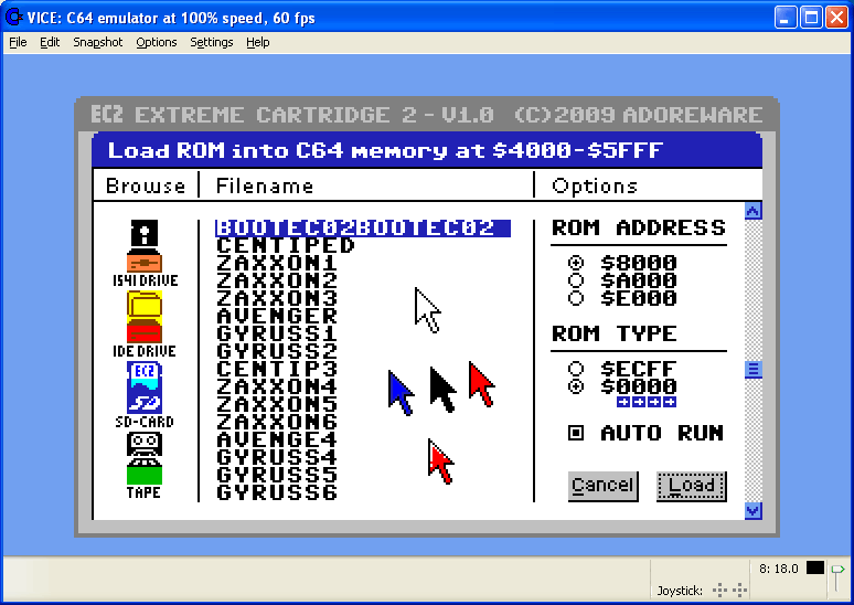 The red-white-black & blue-light-blue-black are triple-layer, the solid black is obviously single, and the rest are double. These are just ideas taken from the Windows cursor. The Amiga cursor would be a good alternative: 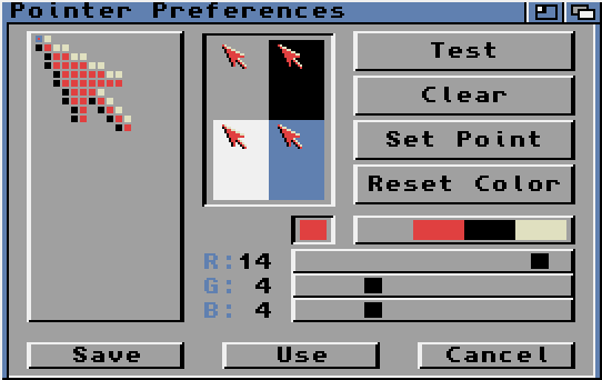  |
|
|
|
Post by Adoreware on Jan 26, 2009 20:25:12 GMT -5
Can I convince you to go with high resolution for the pointer as well? Preferably double-layer (or even triple-layer) sprites, but anything hi-res would be better than multicolor for such a nice hi-res interface. Here's a mock-up: The red-white-black & blue-light-blue-black are triple-layer, the solid black is obviously single, and the rest are double. These are just ideas taken from the Windows cursor. The Amiga cursor would be a good alternative: I started with a hires pointer and already planned to go back. The multicolor is quite bulky. I'm even considering doing away with a pointer to save memory. I'm trying to keep the code within the 16K limit to fit in two 8K ROMs. I have spent hours reducing code and graphics to make room. I have used 12 out of 16K so far, so the pointer may have to go considering so far it is using almost 500 bytes and it only moves around the screen but does not click anything yet. That may tak another 500 bytes??? P.S. Thanks for the multilayer tip, I didn't even think about that. |
|
|
|
Post by Adoreware on Feb 1, 2009 8:48:44 GMT -5
As you might imagine, writing a GUI takes a lot of space and I finally ran out  . I was trying to fit everything into two 8K ROMS, but I failed. I have spent the past three days moving a huge section of the code to a third bank. The bank switching was quite time consuming because I didn't plan ahead. The good news is that all code is now working in the new bank. I also added a 4th bank (not making the same mistake again) in the event I fill up the 3rd. This will total 32K. The bank switching is not like other carts. For VICE developers, there are three 8K banks at $8000-$9FFF and one at $A000-BFFF. Right now, I am using Final Cartrigde III cartridge type so I can continue to use VICE. I just duplicate the $A000-$BFFF ROM in all 4 banks and write $40+bank number to $DFFF to switch banks. Once I finish, I will provide the VICE team the EC2 registers so they can support the EC2 if they want. I have completed the Flash erase routine. I added functions to display Message Boxes, Prompt Boxes, and the Progress Bar. The software now loads an 8K ROM into the C64 memory at $4000-$5FFF. Hard Drive, SD-CARD, and Cassette will follow. Right now, I am moving onto writing the contents of $4000 to the flash. Finally!!! Once I get this working, I will be for the most part working mostly with the EC2 board and not the Cyclone II development board. I am very excited to be at this point. Writing to the flash is the final step. I know I can write because erasing is writing and the erase routine erases the flash. I don't want to sound like a broken record, but does anyone have information on the GS38AC325PK01 44 pin IC on the Action Replay V6 cart? If I knew what type of chip it is (CPLD or PLA), I might be able to read the contents. I don't even know what the pin out is. The PLA file already available on various sites is for V5 and is not the same thing. |
|
|
|
Post by saehn on Feb 1, 2009 16:53:16 GMT -5
I don't want to sound like a broken record, but does anyone have information on the GS38AC325PK01 44 pin IC on the Action Replay V6 cart? If I knew what type of chip it is (CPLD or PLA), I might be able to read the contents. I don't even know what the pin out is. The PLA file already available on various sites is for V5 and is not the same thing. Sorry to hear about the problems with the space but having a little bit extra sounds like it will be so much better. As a bit of incentive, I believe I might have gotten an answer for you on the AR6 question (thanks to Groepaz). Hope this helps! noname.c64.org/csdb/forums/?roomid=7&topicid=63514#63516 |
|
|
|
Post by Adoreware on Feb 1, 2009 21:13:33 GMT -5
I don't want to sound like a broken record, but does anyone have information on the GS38AC325PK01 44 pin IC on the Action Replay V6 cart? If I knew what type of chip it is (CPLD or PLA), I might be able to read the contents. I don't even know what the pin out is. The PLA file already available on various sites is for V5 and is not the same thing. Sorry to hear about the problems with the space but having a little bit extra sounds like it will be so much better. As a bit of incentive, I believe I might have gotten an answer for you on the AR6 question (thanks to Groepaz). Hope this helps! noname.c64.org/csdb/forums/?roomid=7&topicid=63514#63516OK, let me try to explain. First look at this...  The top three photos going left to right are version 6 top, version 5 bottom, version 5 top. The photo on the bottom is also version 5. There are two different version 5s. The earlier version (bottom) has 5 ICs (28S129 PLA, 74LS74, 74LS163, 74LS273, 74LS02) while the newer version (top) has the 44 pin GS38AC325PK01. This chip contains all the logic of the 5 ICs on the earlier board including the 28S129 PLA. Version 6 ONLY comes with the GS38AC325PK01 and is exactly the same as the newer version V board. All three boards have the same Ram (circled in green) and Rom (circled in blue). The only difference is the footprint is PLCC on version 6 and DIP on both version 5s. The schematic I have is for the older version 5 which contains the PLA and as mentioned, I'm not sure if the schematic is correct. I own version 6 and have reversed engineered the schematic, but it does me no good if I don't know the logic inside the GS38AC325PK01. I do understand that there are registers that can be used, but this is not as accurate as reproducing the actual logic in the FPGA. A perfect example is Epyx Fast Load. VICE uses registers, but the character ROM is not visible during disk IO in Vice because there is a delay controlled by a capacitor on the PC board that holds a line hi (or low, I cant remember) for a few micro seconds after IO access. Sorry for the long winded explanation, but the bottom line is that I don't use registers if I don't have to. If the schematic I have doesn't work and I don't have the GS38AC325PK01 logic, then I'm at a stand still. One more thing, the AR5 and 6 are the same hardware wise, but the fastloader is different in the ROM. I have patched ALL ROM versions to use the latest NTSC fastloader (Ver 5). I can do the same for PAL if anyone needs it. |
|


 . I was trying to fit everything into two 8K ROMS, but I failed. I have spent the past three days moving a huge section of the code to a third bank. The bank switching was quite time consuming because I didn't plan ahead. The good news is that all code is now working in the new bank. I also added a 4th bank (not making the same mistake again) in the event I fill up the 3rd. This will total 32K. The bank switching is not like other carts. For VICE developers, there are three 8K banks at $8000-$9FFF and one at $A000-BFFF. Right now, I am using Final Cartrigde III cartridge type so I can continue to use VICE. I just duplicate the $A000-$BFFF ROM in all 4 banks and write $40+bank number to $DFFF to switch banks. Once I finish, I will provide the VICE team the EC2 registers so they can support the EC2 if they want.